

How to Perform PCB Design Review and Layout Clean-Up | Leadsintec
Mistakes occur while designing a circuit board. Performing a PCB design review will help you identify and rectify these errors. During this process, you must analyze and improve board elements such as stack-up, trace, vias, components, and others to ensure zero defects in the layout.
The DRC system can help you avoid some design flaws, but not all of them. Hence, having a final check will enable you to recognize unidentified faults. In this article, we will discuss the review and clean-up process in detail.
How to review a PCB layout?
The evaluation procedure extends to multiple stages of the layout development process:
Before constructing the layout, verify schematic drawings and bill of material (BOM) for the number of netlists and their naming, footprint dimension, assignment of DNI components, polarity, etc.
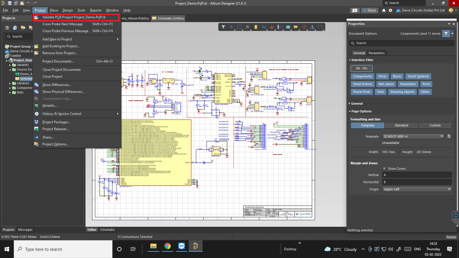
After finalizing the design, visually compare the schematics and constructed circuits to identify any errors. Run a design rule check from the layer stack-up to the component placement. Subsequently, clean up the PCB layout to remove the identified errors.
Finally, check for missing data in the production files before sharing them with the fab house.
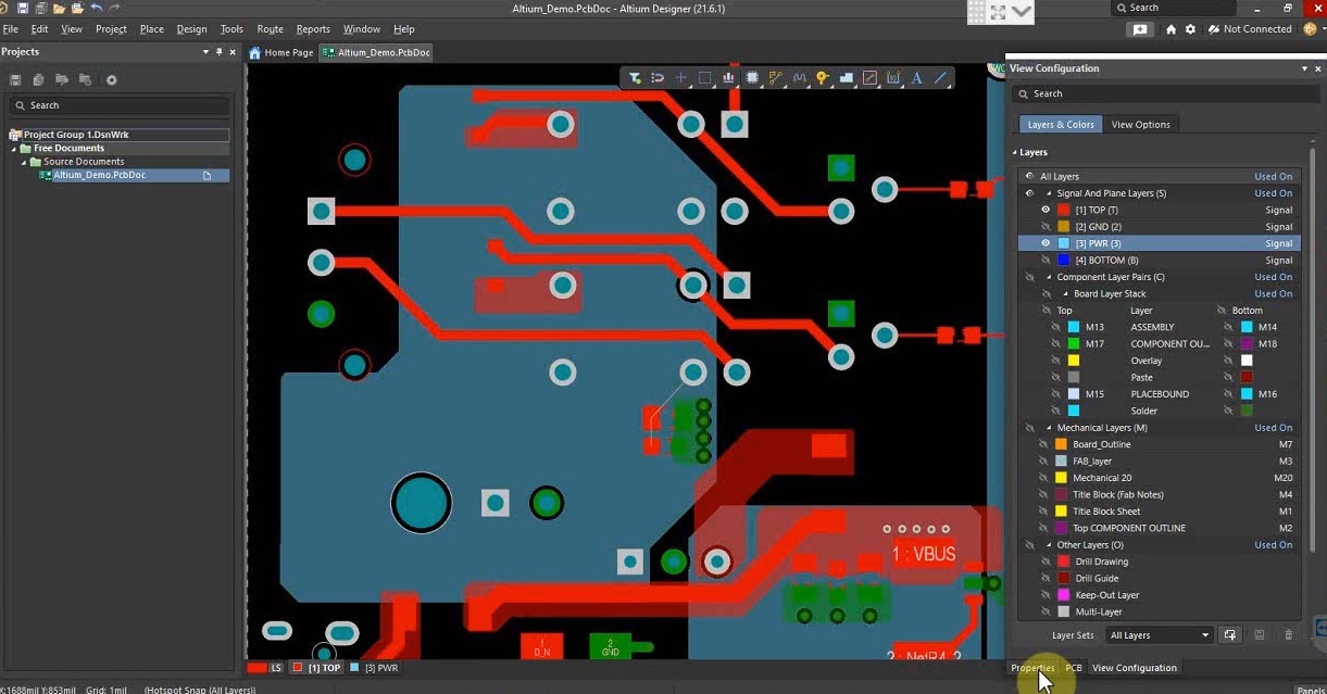
Stack-up plane design and arrangement
The arrangement of ground, signal, and power layers is essential to produce an accurately functioning circuit. Therefore, consider the following points for efficient propagation of the signals.
- Always incorporate a solid power layer.
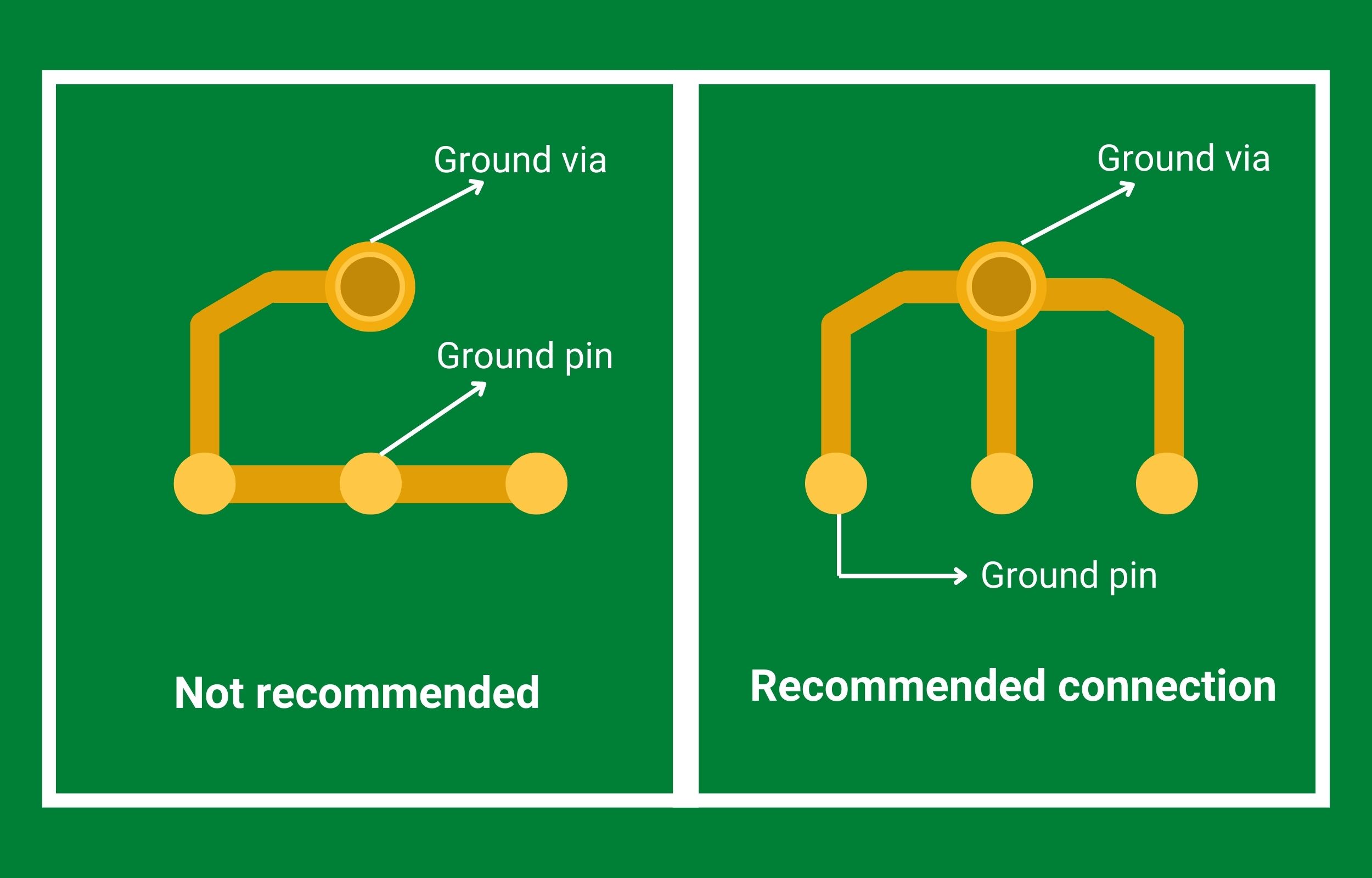
- A single unbroken ground plane should be present in the build-up. Make sure you connect all the ground points to this plane through vias.
- It’s ideal to have separate via for every ground and voltage pin. However, if this is impossible, check if you have individually connected them to the hole, as shown in the image below.
- Avoid placing signal layers adjacent to each other.
- There should be symmetry in the stack-up arrangement to avoid warping.
- Remove the unwanted layers that design tools usually add.

Board dimension checks
- If you plan to install the circuit board in a casing, ensure its dimensions meet all the requirements.
- Check for optimum clearance, at least 10 mils, between the copper trace and the board edge.
- All non-plated holes, including mounting holes (minimum hole diameter of 3.3 mm), should have anti-pads. Additionally, the screw head/nut size should be greater than the diameter of the hole.
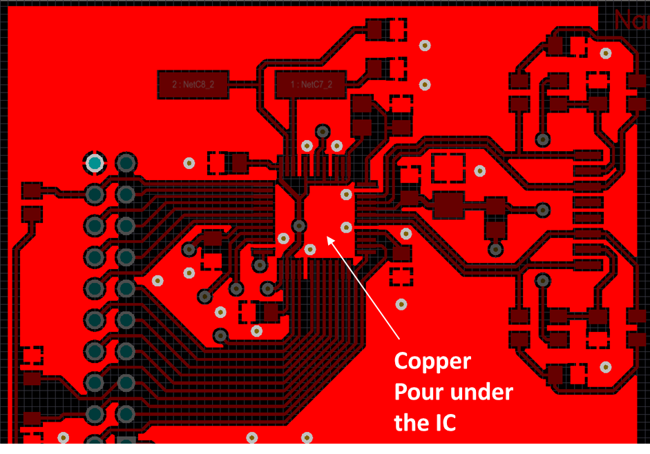
Placing polygons structures
Polygons (copper pours) are the areas around the components or traces filled with copper. They are created only on signal layers.
Ensure no floating copper pours are present in the layout while performing the PCB design review. If they are present, connect them to the ground plane. Furthermore, make sure that they do not create any open nets. If needed, place polygons in other layers to balance the copper distribution in the stack-up.
Reviewing trace placement in the board design
- Calculate the impedance and current carrying capacity of the trace and optimize their width accordingly.
- The length of the signal line and return path should be minimal to reduce noise and improve signal integrity.
- Ensure no open nets are in the circuit. If you want to keep an unconnected line, its length should be as short as possible.
- Maintain sufficient clearance between the traces to suppress crosstalk. Based on the copper weight, the optimum spacing is mentioned in the below table:
| Copper weight | Outer layer trace spacing (in mils) | Inner layer trace spacing (in mils) |
|---|---|---|
| 5 microns | 3 | 2 |
| 9 microns | 3 | 2.5 |
| 1 oz | 6 | 4.25 |
| 2 oz | 8 | 6.25 |
| 3 oz | 12 | 8 |
| 4 oz | 14 | 10 |
- If your traces have formed sharp acute angles (which can go unnoticed in the routing stage) fix them. These can create acid traps. Try to maintain 45° bends.
- Prevent sharp 90° bends, which can cause reflection and distort the signal.
- Make sure that there are no loops in the power and ground net.

 | LEADSINTEC")


