

PCB PROTOTYPING AND TROUBLESHOOTING WITH YOUR MANUFACTURER
As a printed circuit board (PCB) manufacturer for more than 70 years, we have worked with thousands of customers to provide quality products in prototypes of a few pieces to many tens of thousands of circuit boards repetitively.
Each PCB is carefully laid out by our engineering team or theirs. Unfortunately, things happen, and it’s not until the PCB is completely manufactured, assembled, and in the final product that it is discovered the circuit board is not working correctly. What now?
Circuitry too close to the actual PCB edge can be damaged or severed by tooling breakaways and cause delamination.
Unintended PCB Errors
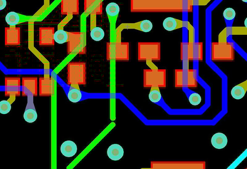
Like most anything, some of the time things can go wrong during the layout and routing phase. Shorting or opens are two of the more common issues. A short is an unintended electrical connection between two points and an open is an unintended break between two points. Either can disrupt the functionality of the printed circuit board’s final product.
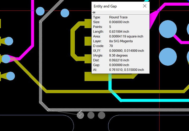
I want to briefly discuss the importance of providing a netlist, preferably an IPC-356 format to your PCB manufacturer with your Gerber package. You can and should request a netlist from your design team to be provided with your deliverables. The netlist is a database of electrical connections that maps and confirms the Gerber files are correctly laid out and will work as intended in the final product. It is loaded with the Gerber files into the CAM program for verification that the design is correct.
The netlist is also used throughout the CAM process to verify no changes have been made within the manipulation of the data. All CAM, no matter what program is used, has the potential to have a human error. When no netlist is provided, the engineer will extract one from the Gerber files, however, this does not verify the layout and routing are correct as provided. It only verifies engineering has made no errors during CAM.
A netlist file when compared to data can find shorts and/or opens within the routed files.
Netlist Or Gerber Files?
Shorting or opening in a PCB some of the time cause the part to be scrapped and redesigned by the design team. In many cases, this costly error is found too late to save the part. When the error is found at assembly, usually something can be done to save the part from being scrapped.
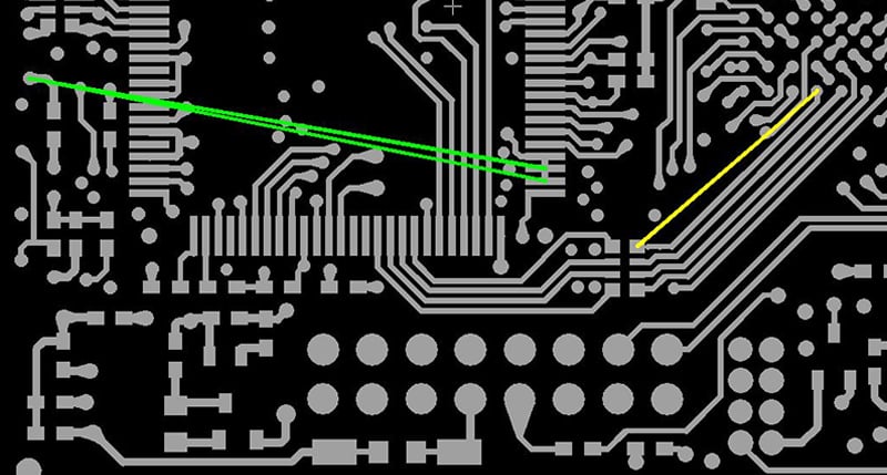
For example, a short between two unintended points can be managed by cutting the connection. The cut is usually done by digging through the protective solder mask layer with a knife-like object down to the circuit and then cutting the copper. Once the copper track is broken, it can be checked with a meter to be sure the cut is clean through. It is an unsightly mess, but it does work. Often touchup in the area with mask is needed to protect the copper that has been exposed from shorting to components or exposure to elements.
An open between points is another issue managed by adding a jumper wire to the PCB. Once the open is identified, often a wire can be hand soldered to the points to engage the disconnect. In both cases, this adds time and cost of materials and labor to save the parts from being scraped. Providing a netlist could have prevented both issues from happening.
Broken traces can also be found when a netlist is provided.
Managing Errors After PCB Manufacturing
So why are we talking about this? Well, in many cases the cost of prototyping and troubleshooting the product and remaking the part is top heavy in cost. During the prototype phase of the PCB, there are options that will allow for some savings while the product is proofed.
Going back to the drawing board of design and layout is not always needed. Sure, some of the time there isn’t a way around it due to certifications and we aren’t suggesting skipping, but some of the time tweaks can be made through an approval process at your PCB engineering level.
We can and have worked with many customers to do just that. A trace cut or add, a clearance or thermal connection add can be completed easily and cleanly. Doing this versus a complete revision is much more cost-effective than a complete re-spin. Documenting the process through an approval is sufficient during prototyping, through an ECN fixing the data set and creating a completely new version or bumping the revision is inexpensive and accurate.
Summary
Clearly, your printed circuit board supplier is an asset when it comes to making a cost-efficient change, documenting the process, and supplying a modified complete data set for your records will save you cost and time to production. Consult your PCB supplier on making corrections to prototypes or those old jobs you have been cutting traces or adding jumpers to parts for years.


 Services | LEADSINTEC")


